2:47
DFN2020B(WF)封装采用可焊锡侧翼引脚结构,可通过AOI设备确认可焊性。与SOT-23F封装相比,该封装在实现高散热性的同时,减少了约43%的贴装面积。
The purpose is to provide various design information for IH cooker and reduce the effort required to design according to actual specifications.
2:00
The lineup of LDO regulators that are ideal for mobile devices, etc.
3:16
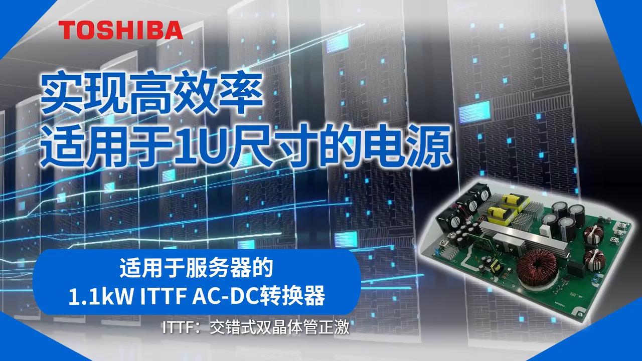
服务器电源对于提高效率和降低损耗至关重要。本参考设计是一款高效服务器电源,采用交错并联双晶体管正激AC-DC转换器(ITTF),输出功率高达 1.1 kW。
3:36
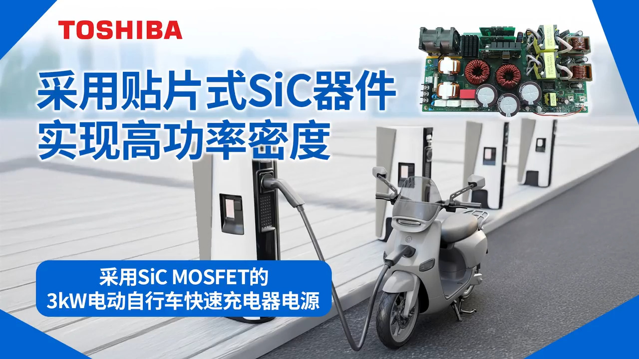
碳中和推动了电动自行车及快速充电的需求增长。此参考设计是一款适用于电动自行车的3kW快速充电器电源。
3:51
该PFC电源采用3相400V交流电(日本以外地区常见)转换为750V直流电。其使用Vienna整流器实现高效的3电平运行,可提供高达5kW的功率。
3:31
为了降低数据中心的功耗,服务器的总线电压越来越多地改为48V。该参考设计为48V服务器提供了一款1.6kW LLC AC-DC转换器,针对1U机架进行了优化,并采用了新一代MOSFET和SiC二极管,以实现高效率和高性能。
3:22